![<?echo $_SERVER['SERVER_NAME'];?>](/template/twentyseventeen/skin/images/header.jpg)
[ Instrument Network R & D ] March 31 news, according to foreign media reports, scientists from the Power and Broadband Gap Electronics Research Laboratory (POWERlab) in Lausanne, Switzerland have produced a high-power terahertz (THz) wave Nano devices. The device does this by generating a powerful "spark" that rises from a peak of 10 V (or less) to 100 V in the picosecond range. A research team led by Professor Elison Matioli said the technology could one day be installed in smartphones and other handheld devices, helping engineers develop faster wireless communications and further the revolution in medical and security imaging systems.
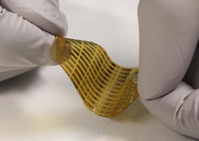
Flexible substrates through which nanodevices can be implemented. Image courtesy of EPFL / POWERlab.
It is reported that terahertz waves have been oscillating at a very high frequency-100 billion to 30 trillion cycles per second, and can penetrate various materials, including wood and stone walls. They can also carry a large amount of data and detect air pollution. Because of these characteristics, engineers and scientists have been trying to use terahertz waves to build future wireless devices. However, traditional electronic equipment can only be switched at a speed of one volt per picosecond, which makes it at least ten times slower than the speed required to generate high-power terahertz waves. Attempts to achieve this have turned into tedious and expensive processes.
In order to make a new nanodevice, Matioli's team separated two metal plates by 20 nanometers, and then applied an incremental voltage to one of them. This caused the electrons on one of the metal plates to surge and form a nanoplasma. Once the voltage reached a certain level, Threshold, the electrons are transferred to another metal plate. The device has an estimated 50 million signals per second, generating a high-intensity pulse that generates high-frequency waves that, when connected to an antenna, can generate, direct, and radiate high-energy terahertz waves.
Researchers explain that obtaining high-energy and high-frequency pulses is an amazing achievement. Because high-frequency semiconductor devices are nano-sized, they can only burst with a few volts. At the same time, high-power semiconductor devices are too large and too slow to generate terahertz waves. To address this, the researchers then decided to combine the principles associated with the old field of plasma with new nanoscale manufacturing technologies.
Researchers say that because terahertz waves are non-ionizing radiation, they do not pose a threat to human health. In fact, the successful use of this technology in the past (if larger and more expensive attempts are made) has resulted in applications related to airport scanning. New research in this area now offers possibilities not only for wireless communication applications, but also for imaging systems developed for healthcare and security purposes. In addition, considering that the construction of these nanodevices is relatively simple, they can be mass-produced at a very low cost.
The lead author of the study, PhD student Mohammad Samizadeh Nikoo, said: "These nanodevices have brought great simplicity and low cost on the one hand, Outstanding performance. Given these unique characteristics, nanoplasma can shape a different future for the ultrafast electronics field. Looking ahead, this technology may be suitable for many applications, including integration with other electronic devices such as transistors. "
Medical Shoe Cover,Disposable Shoe Cover,Surgical Boot Covers,Medical Nonwoven Shoe Cover
Henan Zhongjian Medical Equipment Co., Ltd. , https://www.hnzjmedical.com